Issued Date:2023/7/11 Eg measurement
Issued By:iST
When the mainstream semiconductor material, silicon (Si), cannot meet the demands of high-speed transmission and high voltage, it becomes imperative to find the best wide bandgap material as a replacement. But how do we measure the bandgap? And how do we observe the defects in the crystal stack of the selected wide bandgap material? Eg measurement
In modern life, which heavily relies on mobile or wearable devices, semiconductor materials are omnipresent. From alarm clocks in the morning to electric toothbrushes, ordering breakfast online, watching news on smartphones, and using transportation, work computers, rice cookers, and microwaves for dinner. In recent years, there has been a shift towards cleaner and greener energy sources as a result of the increasing environmental awareness and the necessity to achieve zero carbon emissions. This shift aims to replace the pollutant-emitting oil and gas power generation with more sustainable alternatives. Future tools and technologies will undoubtedly align with this goal and contribute to a cleaner and more sustainable way of life. Eg measurement
Therefore, various high-power and high-speed transmission demands, such as solar energy, wind power, electric vehicles, as well as household appliances, the Internet of Things, and data centers, require new generation materials as silicon (Si), the mainstream semiconductor material, cannot meet these evolving needs. But how are these new materials selected? In this iST classroom will explore the measurement of bandgap and epitaxial quality to discuss how the new generation materials are chosen.
Eg measurement
Eg measurement
1. Why Choose High Bandgap Materials?
With the increasing demand for electrical energy, high voltage, large current, fast transmission, and good heat dissipation are necessary conditions for future new generation materials. Basically, to withstand higher voltage conditions, the energy bandgap (Eg) of the semiconductor material needs to be large enough to tolerate higher critical electric field, achieving stable, fast, and higher-power conversion and output. Eg measurement
The traditional silicon (Si) material has a bandgap of approximately 1 eV, while the compound semiconductors used in handheld mobile devices or fast-charging for automobiles, namely gallium nitride (GaN) and silicon carbide (SiC), have bandgaps around 3 eV, roughly three times that of Si. If we can find materials with even higher wide bandgaps, it will undoubtedly make our lives more colorful.
So, how can we measure the value of bandgap? It can be obtained through two functions available in X-ray photoelectron spectroscopy (XPS)instruments: ultraviolet photoelectron spectroscopy (UPS) and low energy inverse photoelectron spectroscopy (LEIPS), combined with software analysis and calculations.
2. How to Use UPS and LEIPS to Measure the Bandgap?
(a) Ultraviolet Photoelectron Spectroscopy (UPS): Measuring “work function” and the “ionization energy” of semiconductors
UPS mainly uses helium gas (He) as an excitation source, with an energy of approximately 21.12 eV. Compared to the X-ray source (~1 keV) used in XPS, helium gas (He) has a much smaller energy. UPS only interacts elastically with the outermost electrons of the atoms, resulting in a surface-sensitive photoelectron spectrum. Eg measurement
In terms of band structure, the obtained spectrum represents the valence band structure of the outermost electrons of the atoms. From this, the “work function φ” can be measured or the ionization energy (IE) of the semiconductor can be calculated.
(b) Low Energy Inverse Photoelectron Spectroscopy (LEIPS): Measuring the conduction band structure of semiconductor materials
Another method is to use LEIPS to measure the conduction band structure of semiconductor materials, obtaining the electron affinity (EA). As shown in the band diagram on the right in Figure 1, the value of the bandgap in the middle can be easily obtained by subtracting the electron affinity (EA) from the ionization energy (IE).
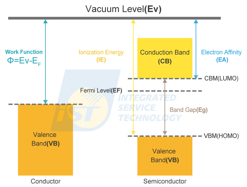
Figure 1: Energy band diagrams of a metal conductor (left) and a semiconductor (right).
(Source: iST Material Analysis Laboratory)Therefore, through these two functions, we can obtain the value of the bandgap of our new material.
In the development of a new type of Ga2O3 device, there have been studies on incorporating Nb2O5 to create N-type doped (Nb-doped) β-Ga2O3 crystals. As shown in Figure 2, the work function φ(WF) of Nb-doped β-Ga2O3 is determined to be 4.96 eV through UPS spectroscopy, and the band structure diagram on the right side of the figure indicates a bandgap value of 4.68 eV. Additionally, research has also been conducted on incorporating aluminum oxide (Al2O3) into Ga2O3 to form (AlxGa1-x)2O3 alloy structures, which can further increase the bandgap value.
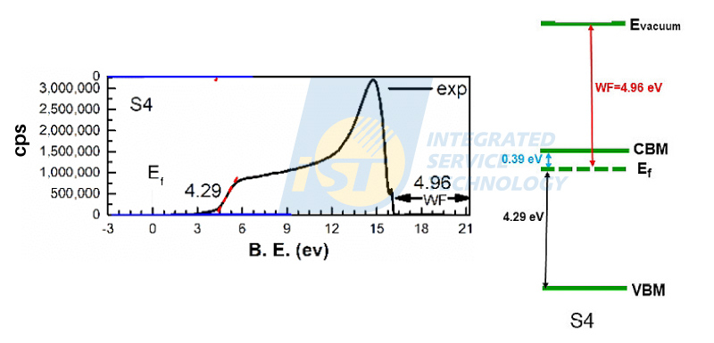
Figure 2: UPS analysis of Nb-doped β-Ga2O3 to derive the bandgap value. Eg measurement
(Ref: Crystals 2021, 11, 135.)Figure 3 shows that when the aluminum (Al) composition x is increased from 0.25 to 0.50, the bandgap is further increased by approximately 0.6 eV. Consequently, the breakdown field also slightly increases, contributing to a greater enhancement in power.
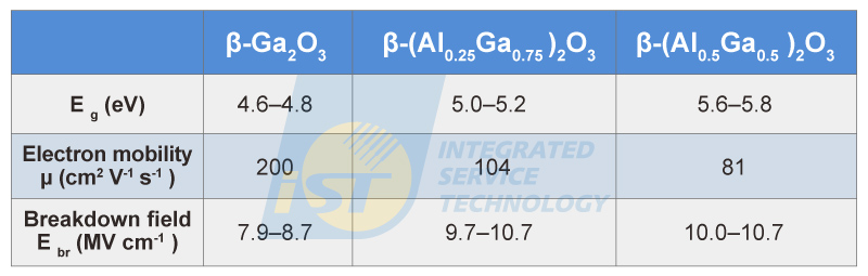
Figure 3: Bandgap and characteristics of β-Ga2O3 & β-(AlxGa1-x)2O3 alloy with x=0.25 and x=0.5.
(Ref: Appl. Phys. Lett. 121, 240503 (2022))3. How Does the Difference in Lattice Stacking Affect the Bandgap? Identification Through XRD
Another characteristic that affects materials is the structure of lattice stacking. Even with the same elemental material, different lattice arrangements can lead to differences in material properties. For example, SiC, which stands for silicon carbide, has over two hundred different crystal forms, with the main three being hexagonal α-6H SiC, hexagonal 4H SiC, and cubic β-3C SiC.
Among them, the 4H SiC structure is most suitable for power device manufacturing. This is because it is easier to fabricate into large wafers and has the highest bandgap and fastest electron mobility.
Figure 4 illustrates the differences in bandgap and critical electric field among these three SiC lattice structures and Si. Similarly, in Ga2O3, a material with a higher bandgap, there are also different lattice structures such as α (trigonal), β (monoclinic), and δ (cubic). Therefore, we need to use X-ray diffraction analysis (XRD) to identify the differences in lattice stacking arrangements in order to select the best materials.
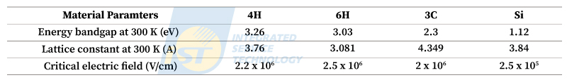
Figure 4: Differences in bandgap and critical electric field between different SiC lattice structures and Si.
(Ref: Crystals 2022, 12, 245)Figure 5 shows the XRD diffraction pattern of Ga2O3 thin film grown on an Al2O3 substrate, and it has been confirmed to be the monoclinic β phase through comparison with the ICDD PDF Pattern (database number: 01-082-3838). The preferred orientation is (211).
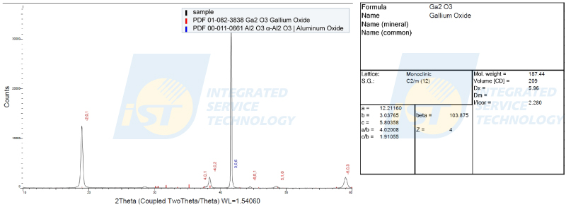
Figure 5: XRD analysis results confirmed that the Ga2O3 thin film on Al2O3 substrate is the β phase of monoclinic crystal structure.
(Source: iST Material Analysis Laboratory)4. How to Observe Crystal Stacking Defects and Imperfections? Relying on XRD and AFM
Once the most suitable material is selected, the fabrication of devices can begin, and various thin films can be stacked on the surface. These films can be the same material, such as epitaxial drift layers on SiC or Ga2O3, or different compound materials, such as GaN epitaxy on Si or SiC substrates. Due to the mismatch in lattice constants, imperfect bonding, dislocations and defects may occur. Eg measurement
The quality of epitaxy can be analyzed and identified through XRD rocking curves and the shift of Raman spectroscopy. Generally, the full width at half maximum (FWHM) is measured to judge the quality. Figure 6 compares the rocking curve overlaid plots of (400)β-(AlxGa1-x)2O3 single crystals grown on seed crystal surfaces with different Al contents (x: 0~0.3). It shows that the FWHM remains stable at 30~50 arc seconds when the Al content is less than 0.3. However, when the content equals 0.3, the FWHM broadens to 150 arc seconds due to the lattice distortion caused by the formation of more internal defects.
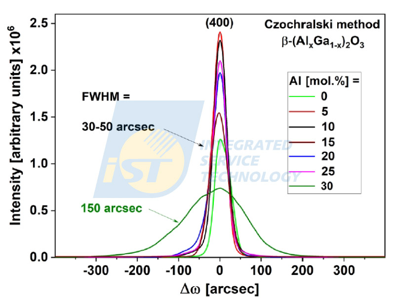
Figure 6: Comparison of overlaid rocking curve plots for single crystal
β-(AlxGa1-x)2O3 grown on (100) seed crystal surfaces with different Al contents (x=0~0.3).
(Ref: J. Appl. Phys. 133, 035702 (2023))In addition, the surface morphology of the epitaxy can be examined by atomic force microscopy (AFM) to determine whether there are stacking defects caused by lattice mismatch or issues resulting from different process conditions.
Figure 7 presents AFM measurements of the surface morphology after epitaxy, showing three typical growth mechanisms: island growth, step flow, and step bunching. These can provide guidance for improving epitaxial process conditions.
However, when observing micro-regions below tens of micrometers in size, cross-sectional scanning electron microscopy (SEM) analysis of samples or focused ion beam (FIB) preparation for observation can be conducted. Transmission electron microscopy (TEM) can also be used to analyze even smaller nanoscale defects, dislocations, and other issues.
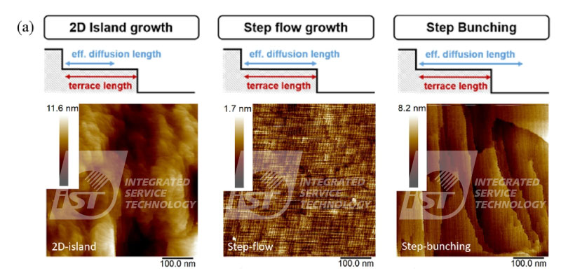
Figure 7: AFM observations of three typical morphologies on epitaxial surfaces: 2D island growth, step flow, and step bunching.
(Ref: Appl. Phys. Lett. 121, 240503 (2022))In recent years, although materials such as GaN and 4H-SiC have been successfully commercialized and demonstrated their superior properties, many studies abroad have begun exploring whether materials such as diamond and boron nitride (BN) can serve as alternative materials to SiC and GaN for power devices. In addition to having higher bandgaps, referred to as “ultra-wide band gap” (UWBG), these materials also exhibit significantly higher thermal conductivity compared to GaN, as shown in Figure 8. This can lead to a 90% reduction in the volume of power modules under rated power, enabling future products to have improved performance that is more readily adopted by the industry.
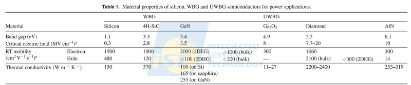
Figure 8: Comparison of properties between ultra-wide bandgap (UWBG) and wide bandgap (WBG) materials.
(Ref. J. Phys. D: Appl. Phys. 53 (2020))Once all the properties of the new generation of materials are confirmed and meet the expected product specifications, the next step is to move towards mass production. This involves processes such as wafer fabrication, device manufacturing, thinning, dicing, wire bonding, and packaging. Subsequently, rigorous reliability verification, lifetime analysis, and failure analysis are conducted. iST can assist you with comprehensive services ranging from backside wafer thinning to packaging, testing, reliability verification, as well as product failure and material analysis.
Moreover, in response to the demand for future automotive electronic products, we also provide reliability verification services for automotive components that comply with AEC-Q standards. We aim to contribute our efforts to the development of next-generation materials and products, ultimately achieving the goal of energy saving, carbon reduction, and a greener planet.
iST Material Analysis Laboratory has been working in the semiconductor and advanced packaging fields for a long time and has accumulated considerable experience and successful cases. If you have any related needs or want to further understand the relevant knowledge, please feel free to contact Chiru Chang at +886-3-579-9909 ext. 6613 or email at sa_tw@istgroup.com;marketing_tw@istgroup.com。